


Signal Integrity analysis
Engineering Domains/SI and PI Simulation
Engineering Domain
Signal Integrity and Power Integrity Simulation
End-to-end SI and PI analysis for package, board, connector, and system-level performance optimization.
SAS performs signal integrity and power integrity analysis across advanced semiconductor hardware platforms to optimize electrical performance and improve system stability.
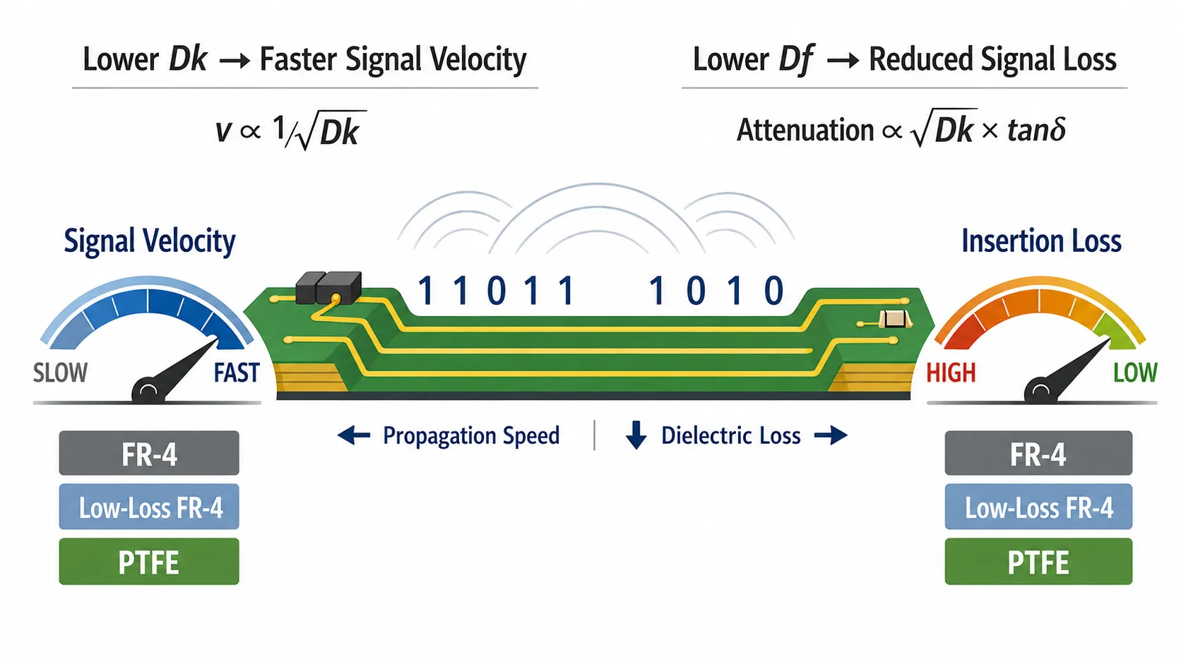
Engineering Capabilities
What SAS Executes in This Domain
06
Capabilities
SAS
Execution CoreSI and PI Simulation
Power Integrity analysis
Eye diagram analysis
TDR analysis
IR drop analysis
PDN optimization
Engineering Model
Decisions That Keep the Program Buildable
Fast risk ranking
Critical nets and power domains are ranked by sensitivity so analysis effort focuses on the paths most likely to affect bring-up.
Model chain discipline
Package models, connector models, board extractions, and device assumptions are kept traceable so results can be challenged and reused.
Analysis tied to layout action
Findings are converted into concrete routing, via, stackup, decoupling, or placement changes instead of isolated reports.
Program Flow
From Definition to Release
Each domain page uses a practical flow that keeps design choices connected to implementation, review, and handoff.
01
Model the target
Collect channel requirements, device models, package data, stackup assumptions, power budgets, and compliance targets.
02
Analyze feasibility
Run topology, loss, impedance, timing, and PDN studies before expensive layout and fabrication decisions are fixed.
03
Extract the implementation
Validate post-layout geometry, vias, planes, return paths, and transitions with extraction-based analysis.
04
Close the loop
Translate results into layout updates, release criteria, and bring-up expectations for the validation team.
Release Package
Outputs Built for Review, Build, and Transfer
SAS structures domain work so the final handoff is practical for engineering review, supplier execution, lab bring-up, and controlled production transfer.
Pre-layout feasibility and topology recommendations
Post-layout SI and PI simulation reports
PDN, IR drop, and decoupling guidance
Action list for layout closure and validation readiness
More Domains
Continue Across the SAS Engineering Stack
Engineering Domain
High Speed PCB Design
Constraint-driven multilayer PCB engineering for high speed compute, RF, mixed-signal, and advanced semiconductor platforms.
Engineering Domain
IC Package and Substrate Design
Advanced substrate and package engineering for high performance semiconductor platforms.
Engineering Domain
112G PAM4 and Advanced Interconnect
High speed serial channel engineering for next-generation semiconductor and compute platforms.
Engineering Domain
Silicon Photonics and CPO
Engineering support for silicon photonics integration, optical interfaces, and high-speed photonic test environments.
Engineering Domain
DFM and Production
Transforming advanced engineering concepts into manufacturable and scalable semiconductor hardware platforms.