


Design for Manufacturability (DFM)
Engineering Domains/DFM and Production
Engineering Domain
Design for Manufacturability and Production Execution
Transforming advanced engineering concepts into manufacturable and scalable semiconductor hardware platforms.
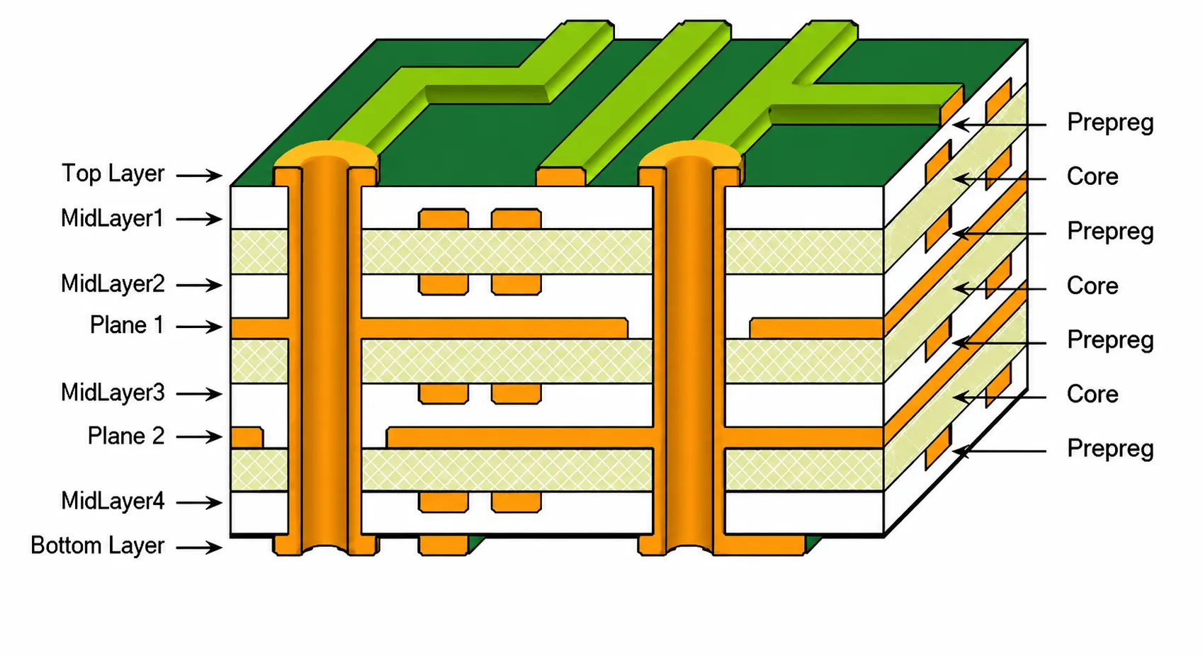
SAS provides full design-to-production execution support, ensuring engineering concepts are optimized for manufacturing, validation, assembly, and long-term production scalability.
Engineering Capabilities
What SAS Executes in This Domain
05
Capabilities
SAS
Execution CoreDFM and Production
Fabrication alignment
Assembly readiness
Production traceability
Validation coordination
Engineering Model
Decisions That Keep the Program Buildable
Build risks surfaced early
Manufacturing limits, supplier rules, tooling needs, and inspection points are reviewed before release data is frozen.
Prototype learning captured
First-build feedback becomes controlled design, process, and documentation updates instead of tribal knowledge.
Ramp path maintained
Sourcing, assembly, test, traceability, and revision control are coordinated so later builds do not restart from zero.
Program Flow
From Definition to Release
Each domain page uses a practical flow that keeps design choices connected to implementation, review, and handoff.
01
DFM planning
Review design intent, supplier path, process limits, materials, tooling needs, and release expectations.
02
Release readiness
Prepare manufacturing files, drawings, BoM data, inspection criteria, and build notes for controlled handoff.
03
Prototype build
Support fabrication, assembly, inspection, test, deviation handling, and rapid feedback into engineering.
04
Production transfer
Convert validated build knowledge into repeatable documentation, supplier control, and sustaining workflows.
Release Package
Outputs Built for Review, Build, and Transfer
SAS structures domain work so the final handoff is practical for engineering review, supplier execution, lab bring-up, and controlled production transfer.
DFM review findings and release action list
Manufacturing package with drawings, notes, and BoM controls
Prototype build feedback and ECO recommendations
Production transfer and sustaining support plan
More Domains
Continue Across the SAS Engineering Stack
Engineering Domain
High Speed PCB Design
Constraint-driven multilayer PCB engineering for high speed compute, RF, mixed-signal, and advanced semiconductor platforms.
Engineering Domain
IC Package and Substrate Design
Advanced substrate and package engineering for high performance semiconductor platforms.
Engineering Domain
SI and PI Simulation
End-to-end SI and PI analysis for package, board, connector, and system-level performance optimization.
Engineering Domain
112G PAM4 and Advanced Interconnect
High speed serial channel engineering for next-generation semiconductor and compute platforms.
Engineering Domain
Silicon Photonics and CPO
Engineering support for silicon photonics integration, optical interfaces, and high-speed photonic test environments.