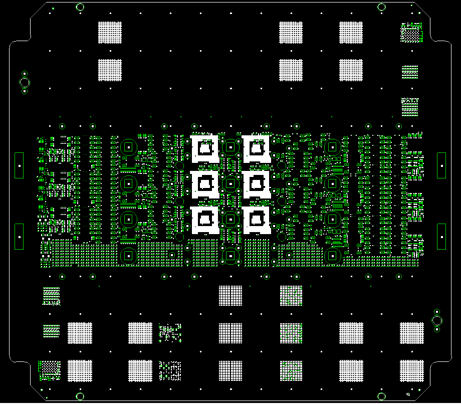
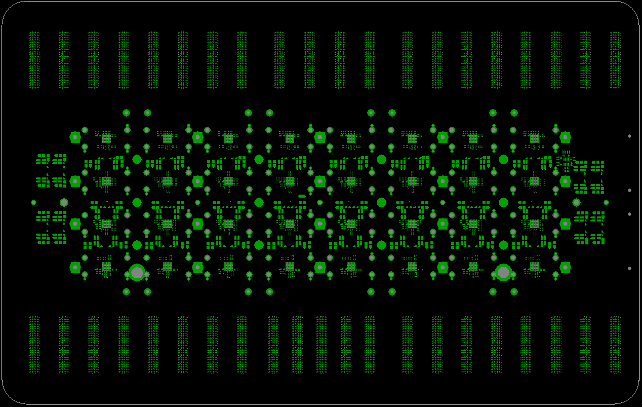
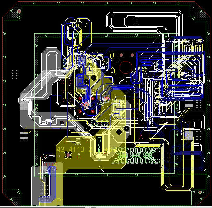
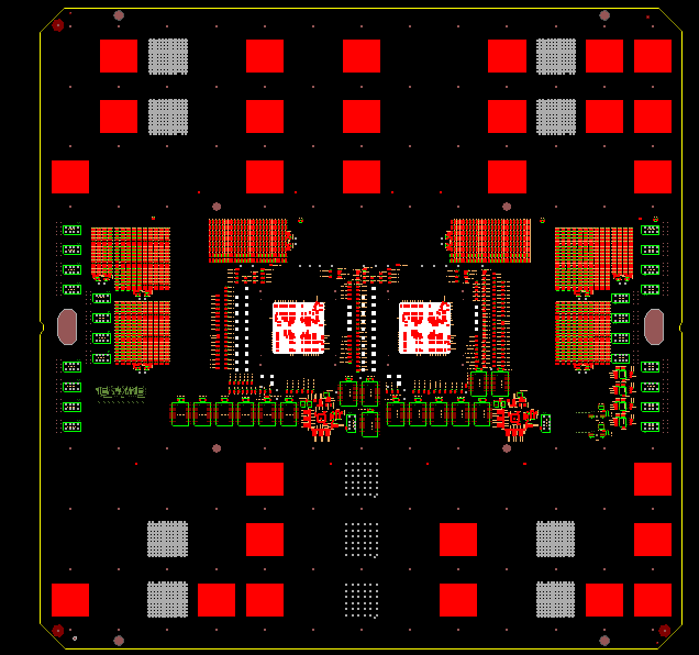
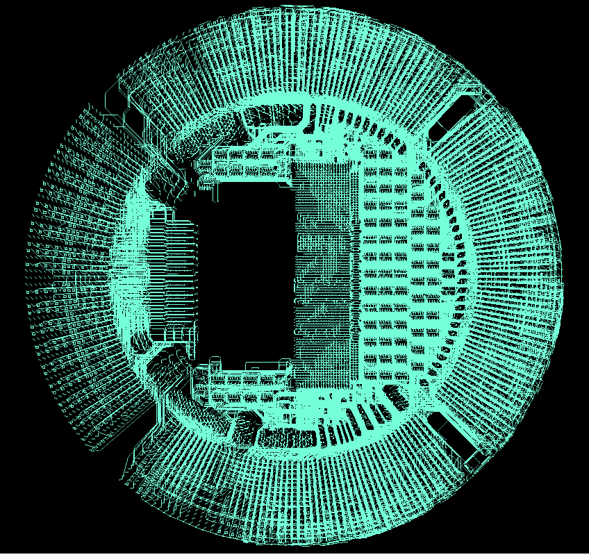
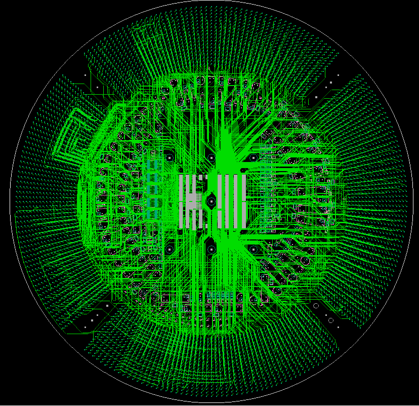
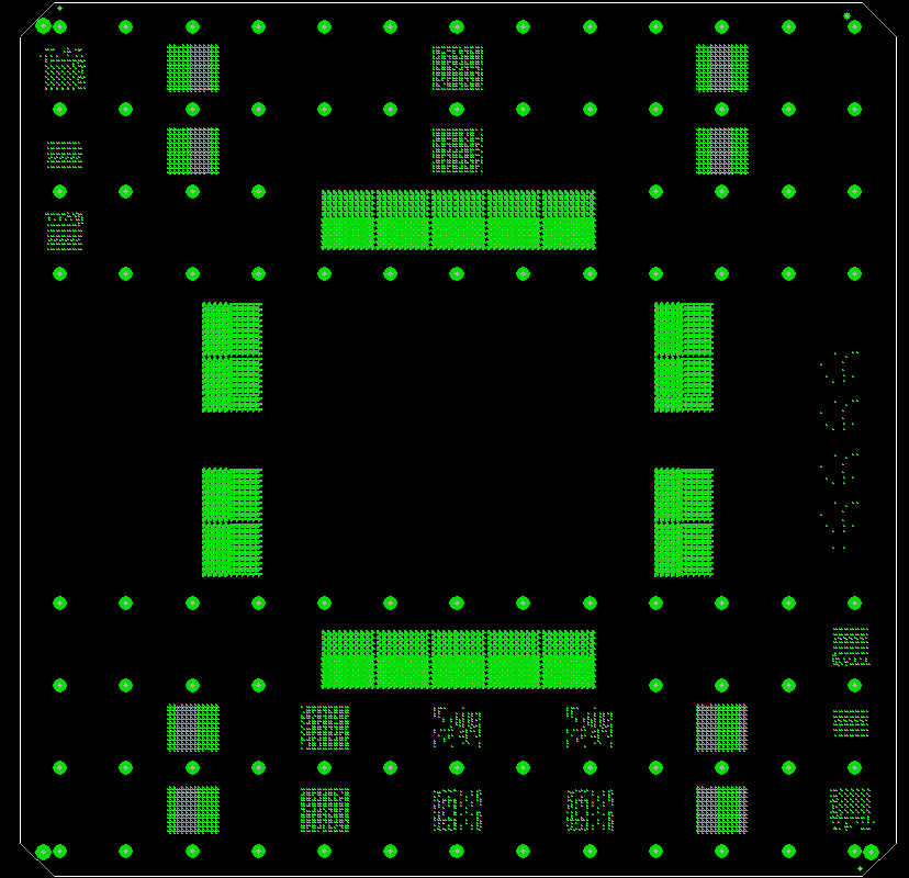
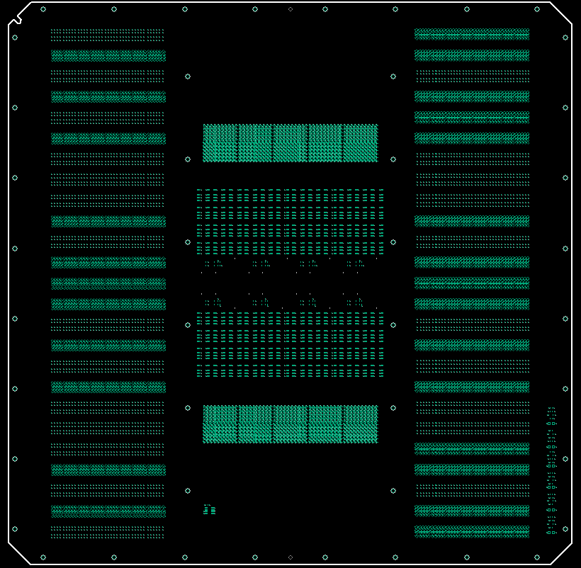
Load Boards
UltraFlex Load Board
IntegraFLEX Load Board
ETS364 Load Board
T2000 Load Board
J750 Load Board
T6573 Load Board
112G Advantest 93K Load Board
RASP Square Load Board
NI STS Load Board
UltraFlex Load Board
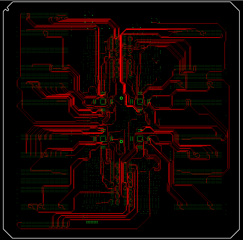
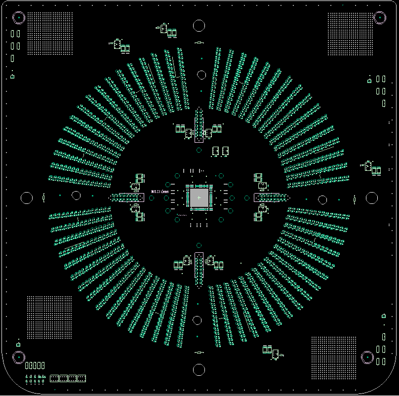
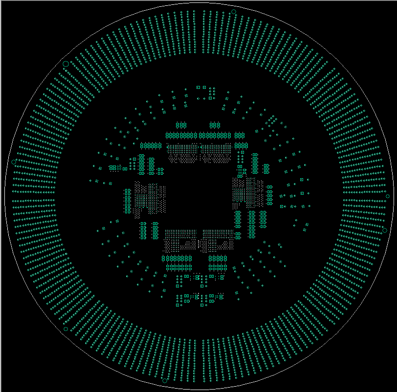
Probe Cards
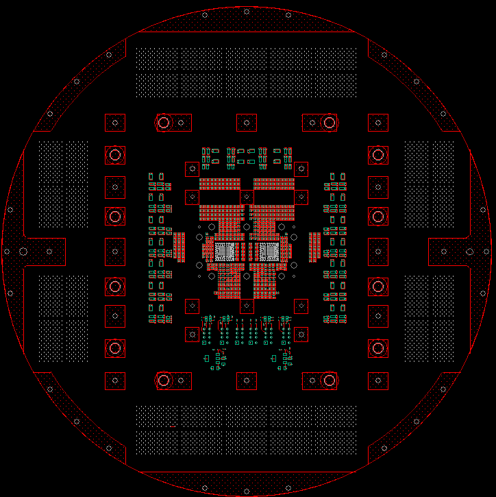
UltraFlex Probe Card
J750 Probe Card
T6372 Probe Card
T6373 Probe Card
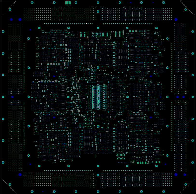
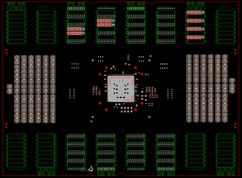
Probe Interface Board
UltraFlex PIB
IntegraFLEX PIB
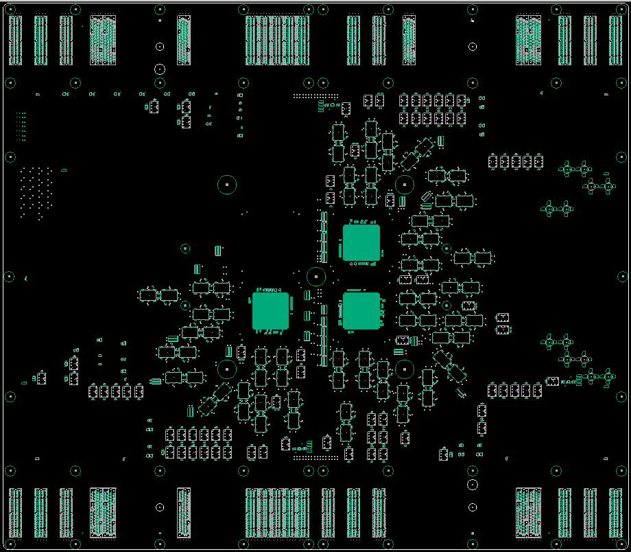
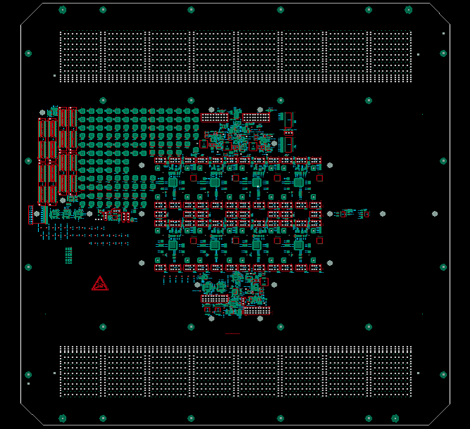
Characterization Boards
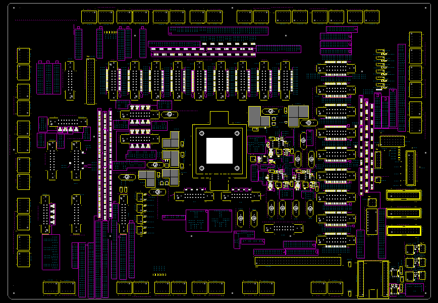
PM8667 Char Board
PM8667 Char Board
Full Turn Key Solution
Post Silicon Engineering
Our process encompasses various stages, each contributing to the successful design and development of integrated circuits (ICs) or chips. Here are the key steps involved in the design process:
Requirement Specification
We begin by thoroughly understanding the customer's requirements and specifications, including the chip's purpose, intended application, performance goals, power constraints, and other design considerations.
Architecture Design
Next, we determine the high-level architecture of the chip, identifying major functional blocks, their interconnections, and the overall system organization. This helps define the chip's functionality and performance capabilities.
Functional Design
Our engineers break down the chip's architecture into smaller functional units, specifying the behavior and functionality of each unit, considering inputs, outputs, and internal operations.
Register Transfer Level (RTL) Design
Our RTL design phase involves representing the chip's functionality using a hardware description language (HDL) like Verilog or VHDL. Our engineers create a detailed description of the chip's behavior at the register transfer level.
Functional Verification
SAS conducts an extensive verification to ensure the chip functions as intended. Techniques such as simulation and formal verification are employed by our teamto test the chip's behavior against specified requirements, identifying and resolving any functional issues or bugs.
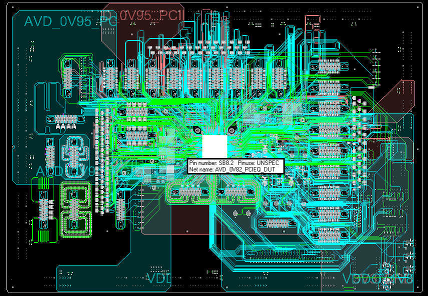
Physical Design
We convert logical design into a physical layout that can be manufactured. This involves tasks like floor planning, placement, routing, and consideration of factors like power distribution, signal integrity, and manufacturability.
Design for Manufacturability (DFM)
Our engineers optimize the layout to ensure the design can be fabricated reliably and cost-effectively, employing techniques such as reducing design variations, optimizing lithography masks, and improving yield.
Tapeout
Our team prepares chip design files for manufacturing by generating a set of files called the tapeout, providing the necessary information for the fabrication facility (fab) to manufacture the chip.
Fabrication and Packaging
The tapeout files are sent to the fab, where the chip is manufactured on a silicon wafer using various processes. After fabrication, the wafer is diced into individual chips, which are then packaged to protect them and provide electrical connections for integration into electronic devices.
Testing and Characterization
Fabricated chips undergo extensive testing carried out by SAS’s expert team which includes functional, performance, and reliability testing. Chips are characterized to determine their electrical characteristics such as power consumption, timing, and signal integrity.
Post-Silicon Validation
Further validation and testing is conducted by SAS team after deploying chips in real-world applications, ensuring performance and reliability in target systems and identifying any system-level issues.
Trusted by companies worldwide